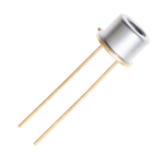
GaN type UV sensors “KPDU086SU27-H11Q and KPDU086SU31-H11Q” achieve high sensitivity to UV-B and UV-C deep ultraviolet rays
TOKYO–(BUSINESS WIRE)–Kyoto Semiconductor Co., Ltd. (President and CEO Yoshihisa Shinya, Head office: Fushimi-ku, Kyoto city), a leading optical device solution manufacturer with world-class technologies and Japanese quality, has announced two products of GaN*1 UV sensor; “KPDU086SU27-H11Q and KPDU086SU31-H11Q”.
The UV sensors “KPDU086SU27-H11Q” and “KPDU086SU31-H11Q” were developed with the aim of achieving higher sensitivity than conventional Si*2 type UV sensors to meet the needs of the deep UV*3 sensing market.
Since conventional Si-type UV sensors detect a wide range of wavelengths, it is common to apply a filter to limit the sensitivity to the UV wavelength range. The amount of light was attenuated by passing through the filter.
The newly developed KPDU086SU27-H11Q and KPDU086SU31-H11Q use GaN to enable direct light reception at the light receiving part of the sensor without using a filter as GaN has sensitivity to a specific wavelength range of ultraviolet light. It is now possible to obtain approximately three times as high sensitivity as Si-type UV sensors. *4
In addition, the products have sensitivity in the wavelength range limited to UV-B*5 and UV-C*6, which are in high demand among ultraviolet rays.
The new products can be used to monitor the ultraviolet light intensity of germicidal lamps in food factories, medical institutions, and water purification-related institutions, and to monitor the light intensity of ozone detection light sources.
The mass production of the GaN UV sensors “KPDU086SU27-H11Q and KPDU086SU31-H11Q” are scheduled to start on April 28, 2023.
For more information
https://www.kyosemi.co.jp/en/products/kpdu086su27-h11q/
https://www.kyosemi.co.jp/en/products/kpdu086su31-h11q/
*1 GaN: Gallium nitride a type of semiconductor
*2 Si: Silicon, a type of semiconductor
*3 Deep ultraviolet rays: UV rays in the emission wavelength range of λ = 200-300 nm. UV-B and UV-C are said to be deep UV rays.
*4 Comparison between KPDU086SU27-H11Q and our Si UV sensor KPDU400F-2
https://www.kyosemi.co.jp/products/kpdu400f-2/
*5 UV-B: Ultraviolet rays in the emission wavelength range of λ = 280 to 315 nm. Sensitivity wavelength range of KPDU086SU31-H11Q
*6 UV-C: Ultraviolet rays in the emission wavelength range of λ = 100 to 280 nm. Sensitivity wavelength range of KPDU086SU27-H11Q
About Kyoto Semiconductor
Kyoto Semiconductor was established in 1980 in Kyoto as a dedicated manufacturer of optical semiconductors. The semiconductors manufactured offer superlative performance and precision, suited for use in optical transmission. They are manufactured end-to-end, including pre- and post-processing, and together with Kyoto Semiconductor’s unique packaging technology, at our location in Japan and made available to customers around the world. Kyoto Semiconductor leads the industry with world-standard technologies for optical device solutions based on Japanese quality and attention to production detail.
Company Website: https://www.kyosemi.co.jp/
*Product names, company names, and organization names mentioned in this press release are trademarks or registered trademarks of their respective companies.
*All contents of this press release are as of the date of publication and subject to change without notice.
Contacts
Media Relations, Kyoto Semiconductor Co., Ltd.
Email: Media_relation@kyosemi.co.jp
The content is by Business Wire. Headlines of Today Media is not responsible for the content provided or any links related to this content. Headlines of Today Media is not responsible for the correctness, topicality or the quality of the content.


